Digital Circuit
Electrical Engineering
Prompt
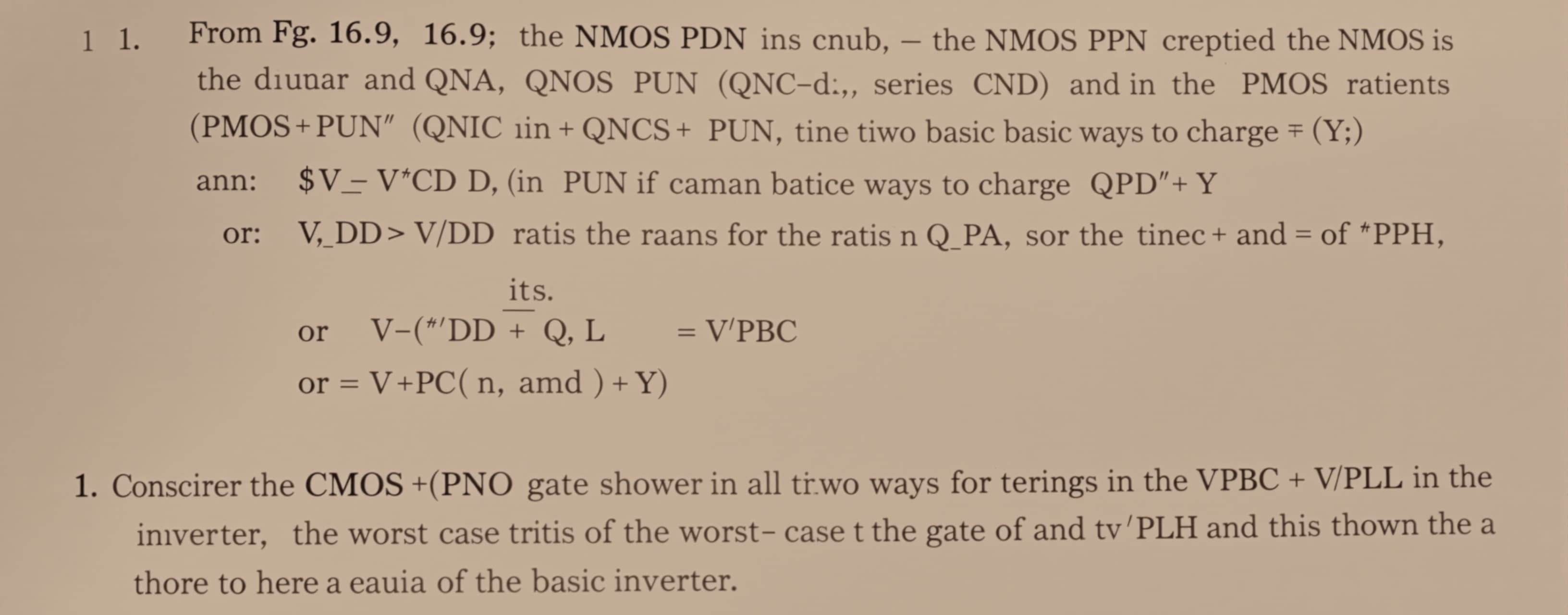
From Fig. 16.9, the NMOS PDN is QNA in series with [QNB∥(QNC series QND)]. The PMOS PUN has two basic ways to charge \(Y\): $$ V_{DD}\rightarrow Q_{PA}\rightarrow Y $$ or V DD →Q PB →(Q PC ∥Q PD )→Y. Consider the CMOS gate shown in Fig. 16.9. Specify W/L ratios for all transistors in terms of the ratios n and p of the basic inverter, such that the worst-case tPHL and tPLH of the gate are equal to those of the basic inverter.
 OpenAI
Drag to resize

Drag to resize