bench
Prompt
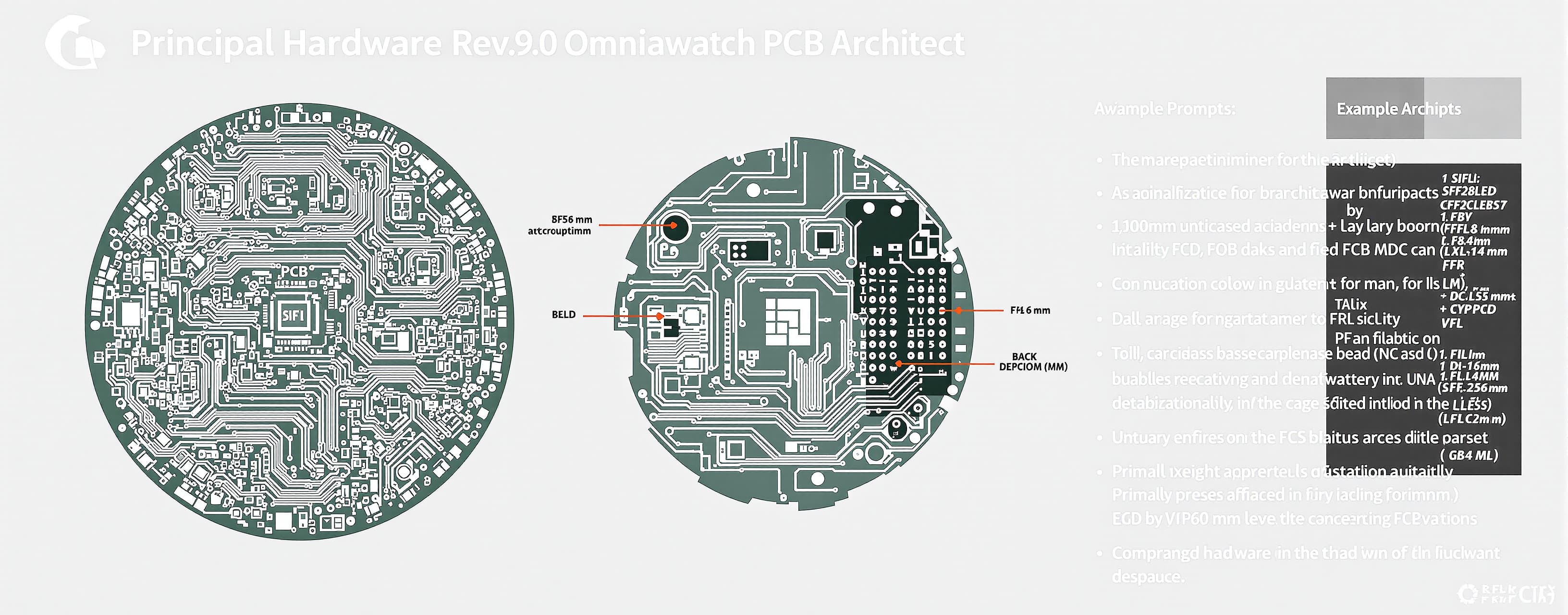
Act as a Principal Hardware PCB Architect. Evaluate the physical PCB feasibility of the Omniawatch Rev 9.0 smartwatch architecture based on the following engineering specifications: - Form Factor Envelope: Circular main PCB with maximum diameter Ø39 mm (surface area ≈ 1194.6 mm² per face). Double-sided SMT assembly. - Target Fabrication Stackup: 8-layer HDI, 0.8 mm nominal board thickness, FR-4 Tg170, ENIG surface finish, 1 oz copper class, 3/3 mil (75/75 µm) minimum trace/space in dense areas, 0.10 mm laser microvias, via-in-pad filled and capped (VIPPO) in BGA zone. Primary target is 1+6+1 HDI; fallback is 2+4+2 HDI. - Major ICs to be placed on the Ø39 mm board: 1. SiFli SF32LB587VEE56 SoC (BGA256, 0.4 mm pitch, 6.5 × 8.5 × 0.94 mm). 2. Kingston EMMC128-TY29 128 GB eMMC 5.1 (11.5 × 13 × 0.8 mm). 3. SiFli SF30147C peripheral PMIC. 4. TI BQ25180 1S LiPo charger / power-path IC (DSBGA-8). 5. Analog Devices MAX17262 fuel gauge (WLP-9, 0.4 mm pitch, 1.5 × 1.5 mm). 6. u-blox MIA-M10Q GNSS module (4.5 × 4.5 × 1.0 mm). 7. STMicroelectronics ST54L NFC controller + Secure Element (WLCSP90). 8. Bosch BMI270 6-axis IMU (LGA-14, 2.5 × 3.0 × 0.8 mm). 9. Bosch BMM350 magnetometer (WLCSP, 1.28 × 1.28 × 0.5 mm). 10. Micro Crystal RV-3028-C7 RTC (3.2 × 1.5 × 0.8 mm). 11. 48 MHz and 32.768 kHz crystals, board-to-flex connectors for display and rear satellite, RF matching circuits, passives. Provide a rigorous technical review addressing: 1. Feasibility of BGA256 0.4 mm pitch escape routing on a 1+6+1 HDI stackup versus necessitating 2+4+2. 2. Signal integrity and reference plane allocation across the 8 layers given simultaneous routing of MIPI-DSI, eMMC, USB 2.0 High-Speed, RF feeds, and switched power rails. 3. Warpage, mechanical rigidity, and thermal expansion risks for a thin 0.8 mm circular board under double-sided reflow. 4. Concrete layout recommendations to prevent high-density routing bottlenecks between the central SoC and the large 11.5 × 13 mm eMMC package.